Our Services

Expertise in designing and fabricating gain chips, lasers, External Cavity Lasers, High power Single Mode Lasers, Semiconductor Optical Amplifiers (SOAs), photodetectors, solar cells, FETs, field effect transistors, diodes and more.
Device Modeling and Simulations, Mask layout, Epi-design and procurement, fabrication process development, chip testing Ray Trace Analysis - Zmax or Light-tools - Solid works package layout - Prototype Optical Packages
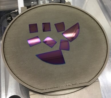
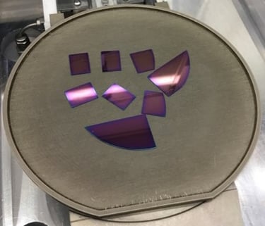
Offering etching, Bragg Gratings (III-V) metalization, wafer lapping, polishing, and thin film deposition for advanced semiconductor devices.
Thin film deposition, Diffusion, Metalization, Reactive Ion Etching, Wet chemical etching, Photolithography, Mask Layout and Design and test, Wafer Lapping and Polishing, Wafer Cleaving and chipping - Optical Coating Services.
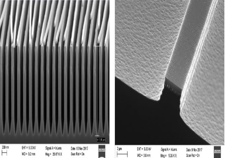
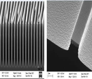
Process Characterization: Scanning Electron Microscopy, Microscopy, Profilometry, Ellipseometry,
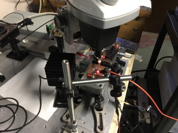
Device Characterization: Power vs Current Vs Voltage (PIV) pulsed and cw Far-field, Near-field Modal Analysis, Spectrum, Polarization Extinction Ratio
Comprehensive Chip Testing for Design Optimization- Prior to Packaging
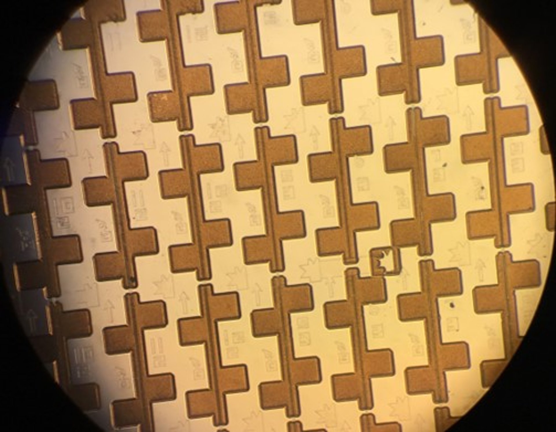
Semiconductor Processing III-V and Silicon
Device Fabrication -Process Multiple Samples Per Run for Cost-Effective Design Optimization
We design, fabricate, and test custom photonic devices and provide comprehensive semiconductor processing and characterization.
Design Prototype and Test Application Specific Semiconductor Devices